Revolutionizing Semiconductors: The Future of Chipmaking and the End of Moore's Law
The world of semiconductors is entering uncharted territory. For decades, chips have gotten faster, smaller, and cheaper—a trend famously captured by Moore's Law, predicting that the number of transistors on a chip would double roughly every two years. However, the industry is hitting a wall. Transistors, the tiny switches inside chips that allow computers to process information, are becoming so small that it's hard to keep making them any smaller. The solution? Thinking differently about how chips are built and how we power the devices of the future.
The Semiconductor Market Today
The global semiconductor market reached $600 billion in 2025 and is projected to hit $1 trillion by 2030. AI chips alone are growing at 40% annually, driving unprecedented demand for advanced manufacturing.
🇳🇱 ASML's High-Tech Machine: Writing in Light
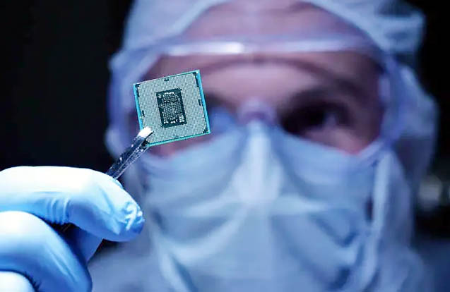
In the heart of Eindhoven, Netherlands, a technological marvel is quietly reshaping the semiconductor landscape. Inside ASML's state-of-the-art facility, a massive 150-ton machine is taking on one of the most pressing challenges: fitting more transistors onto a chip without pushing the limits of physics. This machine uses extreme ultraviolet (EUV) lithography, an advanced form of etching circuits onto silicon wafers using light. Each second, it fires 50,000 droplets of molten tin, heated to a temperature hotter than the surface of the Sun, creating plasma that emits the needed light. This light writes the designs for the next generation of microchips.
EUV Lithography Explained
EUV (Extreme Ultraviolet) lithography uses 13.5nm wavelength light—much shorter than the 193nm used in previous methods. This allows chipmakers to print features smaller than ever before. ASML is the only company in the world that manufactures these machines, with each unit costing over $200 million.
Why does this matter? It's not just about packing in more transistors. It's about keeping pace with the explosive growth in demand for everything from AI algorithms to smartphones, and even your car's computer system. ASML's technology is helping make that happen by ensuring the industry can continue to make chips that are powerful enough for the tasks of tomorrow.
📉 The End of Moore's Law: A Shift in Strategy
For decades, the industry has relied on Moore's Law to guide innovation. The logic was simple: smaller transistors, better chips. But as transistors shrink to nanometer scales—think smaller than the wavelength of visible light—problems arise. Quantum effects begin to mess with the transistors, causing them to leak power and heat up, limiting their efficiency. The industry now faces a choice: how can we keep chips powerful without shrinking transistors further?
From Planar to FinFET to GAA
- Planar Transistors (pre-2011): Flat, 2D design. Reached physical limits at 20nm.
- FinFET (2011-2024): 3D fin-like structure. Used from 22nm down to 3nm.
- Gate-All-Around (2025+): Nanosheet design with 360° gate control. Enables 2nm and beyond.
Companies like Intel, Samsung, and TSMC are shifting focus. Instead of just making transistors smaller, they are making them more efficient. Designs like FinFET (transistors that look like fins rising out of the silicon) allow for better control of electricity flow, reducing leakage and improving performance. Even newer designs, such as "Gate-All-Around" transistors, surround the conducting channel on all sides, offering even more control and efficiency.
🔬 New Materials and 3D Chips: A Revolutionary Approach
The future of semiconductors might not even involve silicon. Materials such as molybdenum disulfide and carbon nanotubes are being tested as alternatives. These new materials are just a few atoms thick, meaning they can offer better performance and reduce leakage. Carbon nanotubes, for example, allow electricity to flow more freely, making transistors faster and more efficient.
3D Chip Stacking
Companies are moving beyond flat, 2D chips and experimenting with stacking transistors in 3D. This innovation allows for more transistors to be packed into a smaller space without the need to shrink them further. Intel's Foveros, TSMC's SoIC, and Samsung's X-Cube are leading the way in 3D integration.
📊 Key Players in Semiconductor Innovation
| Company | Key Technology | Node (2025-2026) |
|---|---|---|
| TSMC | N2 (2nm) with GAA | 2025-2026 |
| Samsung | SF2 (2nm) + 3D stacking | 2025 |
| Intel | Intel 20A (2nm) + RibbonFET | 2024-2025 |
| ASML | High-NA EUV (0.55NA) | 2025-2026 |
💡 Why It Matters to You
All of this sounds highly technical, but here's why it matters. Your smartphone, laptop, gaming console, and even your car all rely on semiconductors. As we move into an era dominated by AI, cloud computing, and smart devices, the demand for faster and more efficient chips is skyrocketing. The advancements happening now are what will make future technologies possible—whether it's self-driving cars, real-time language translation, or incredibly powerful AI systems that can solve problems we can't yet imagine.
What's Working
- EUV lithography enabling 2nm nodes
- 3D stacking increasing density
- New materials showing promise
- AI driving custom chip design
What's Challenging
- Rising manufacturing costs ($20B+ per fab)
- Quantum effects at small scales
- Heat dissipation in 3D stacks
- Supply chain vulnerabilities
🔮 What's Next: Semiconductor Industry Predictions 2026-2030
- 2026: High-NA EUV machines enter mass production (2nm and below)
- 2027: First commercial carbon nanotube transistors
- 2028: 1,000-layer 3D NAND flash memory
- 2029: AI-designed chips outperform human-designed equivalents
- 2030: $1 trillion semiconductor market; chiplets become standard
The semiconductor industry is on the cusp of a new era. The technologies being developed today will shape the future of not just electronics but nearly every aspect of modern life. While the challenges are immense, the industry is finding new ways to innovate, ensuring that the devices of tomorrow will be faster, smarter, and more powerful than ever before.
In the coming years, we will likely see chips powered by materials that don't even exist in your devices today. As engineers and scientists continue to push the boundaries of what's possible, expect the world around you to change faster than ever. From AI-driven innovations to the next generation of consumer electronics, the world's reliance on semiconductors isn't fading anytime soon—it's only growing stronger.